
Bart Dierickx (Co-Founder and CTO) and Ajit Kalgi (Senior Analog Designer) invented a method to increase the charge collection, thus image lag, of a very long narrow photodiode. The N-type pinned photodiode (PPD) itself is constant in width and homogenous in concentration. It is squeezed between two P+ regions, that are at variable distance from the photodiode (Figure 1).
The presence of the P+ region affects the potential in the photodiode, and the construction is so that the potential drops evenly and monotonically, so as to have an effective electric filed in the photodiode that collects the charges (Figure 2).
Read more about this patent and other CMOS imaging solutions and inventions right here
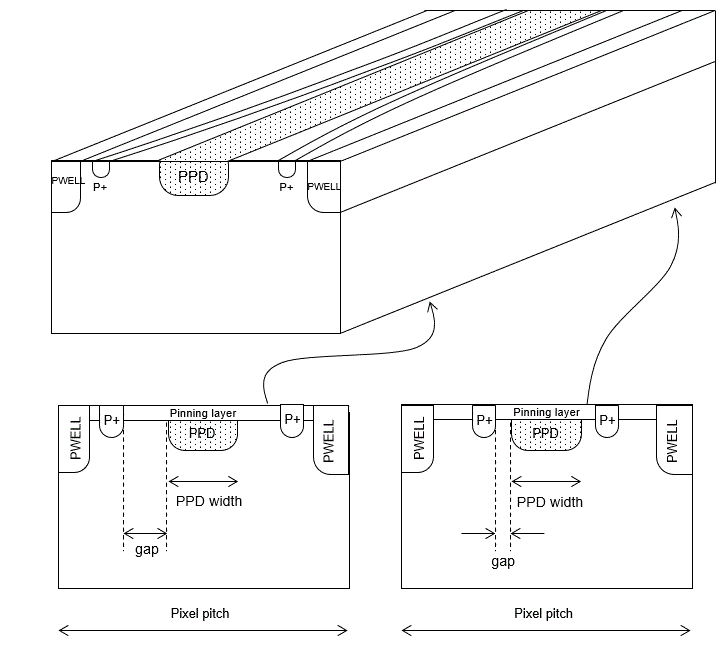
Figure 1
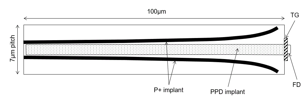
Figure 2
New CMOS imaging technology by Caeleste: gradient photodiode