
| 2022 | US011463634B2 | Granted 20221004 | Charge Domain Binning in a MOS Pixel | 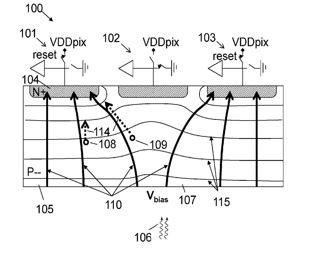 |
| 2022 | US011330207B1 | Granted 20220510 | High Dynamic Range in Direct Injection | 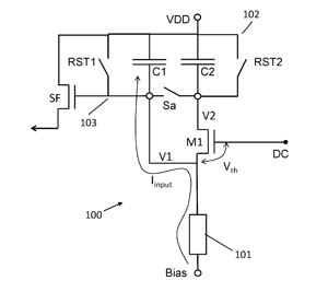 |
| 2020 | BE2019/5067 | Granted 20200828 | Gradient Photodiode | 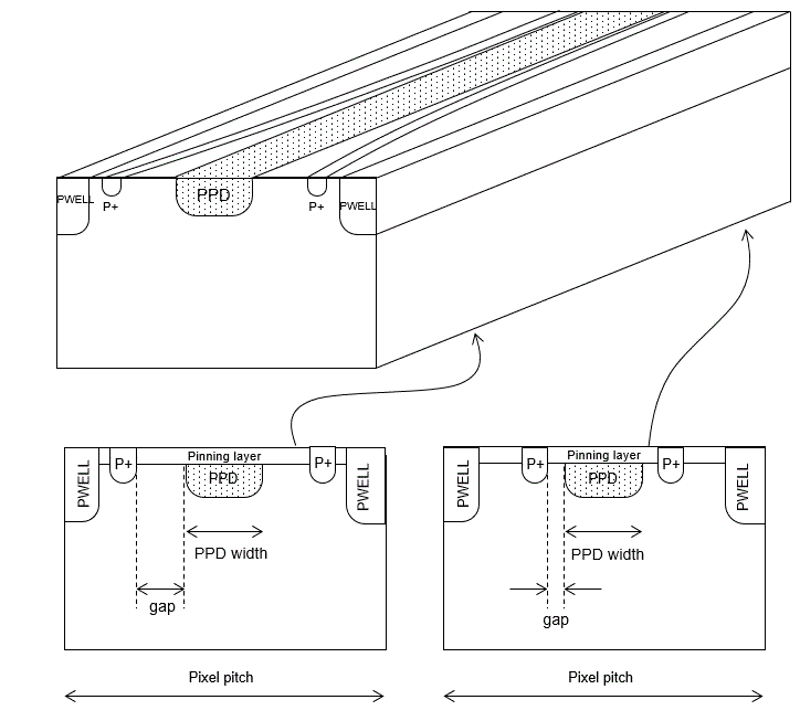 |
| 2020 | US10284824 | Granted 20200407 | Slicing method to detect radiation in an array of pixels and reading out only the pixels or groups of pixels that contain information. | 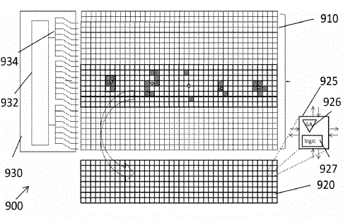 |
| 2020 | US10497737B2 | Granted 20191203 | Enhanced Dynamic Range Imaging |  |
| 2017 | US10284824 | Granted 20190507 | 3D integration of an image sensor and a photonics layer |  |
| 2016 | BE1023468 | Granted 20170329 | Global shutter high dynamic range and 3 level TG. The 3-level TG method extended to pixels in “global shutter” technology, having the extra implants to create a charge domain global shutter. The huge QFW charge for the high dynamic range is not routed via the GS implanted area, but is collected separately by overflow TGs. |  |
| 2016 | US9819882B2 | Granted 20171114 | Global shutter high dynamic range sensor. The 3-level TG method extended to pixels in “global shutter” technology, having the extra implants to create a charge domain global shutter. The huge QFW charge for the high dynamic range is not routed via the GS implanted area, but is collected separately by overflow TGs. |  |
| 2015 | US9699398 | Granted 20170704 | Pixel with increased charge storage. A variation on the theme of high dynamic range imaging by integration on two or more ranges, simultaneously. The large in-pixel capacitor is created is by placing it on top of the PPD as a poly-pinning layer capacitor. | 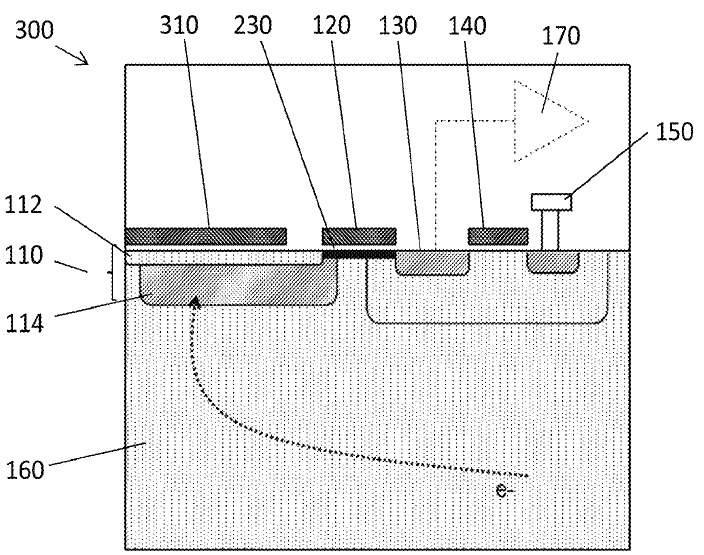 |
| 2014 | US9780138 | Granted 20171103 | High dynamic range pixel by 3-level TG. A dynamic range exceeding 100dB, being fully linear, being compatible with CDS, is reached by the fully synchronous integration of the light on 2 or more “ranges”, each range being of normal dynamic range | 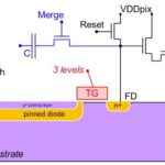 |
| 2011 | JP5864204 | Granted 20160108 | Time gating pixel improved to have multiple collecting diodes. In this improvement the array of “real” photodiodes is subdivide in subarrays that each can have a different effective sensitive / non-sensitive time. Such allows e.g. TOF with lesser frames. | 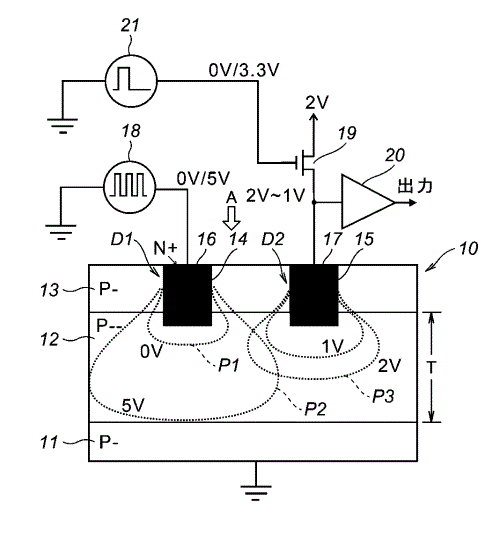 |
| 2011 | US8426828 | Granted 20130423 | Combination of integration and photon counting (X-ray and non X-ray). The duality counting versus integration is soveld: this method patent describes pixels that reuse the same photocurrent that make the counting pixel count in to charge integration. It is applied not only to X-ray or particle detection. Also SPAD-like structures can have combined counting and integration. |  |
| 2011 | US8969780 | Granted 20150303 | TDI in CMOS Although CMOS and not even pinned diodes cannot emulate the genuine TDI operation as CCDs can, this patent solves the issue that CMOS emulations of TDI suffer from MTF loss in the direction of motion. One exploits the capability of a “pinned diode shared pixel” to have partly overlapping integration times for neighboring sub-diodes of a TDI unit cell. An MTF performans as of genuine TDI CMOS can be reached. | 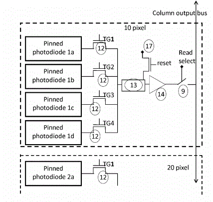 |
| 2010 | BE1021245 | Granted 20150922 | Method to reduce 1/f noise by cycling between accumulation and inversion. In the McWorther interpretation of 1/f noise, it is originating in MOS “interface states”, each of them creating a “RTS” (random telegraph signal) noise. Each interface state has its own capture and release time constant, which acts as a long term memory. The average over a large collection of RTSs yields the 1/f noise spectrum. The technique removes the low frequency part of the noise by periodically cleaning up the long term memory by fording all interfaces states to a majority carrier-filled state by pulsing the MOSFETs in accumulation. | 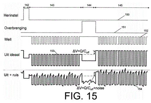 |
| 2009 | US8440957 | Granted 20130514 | Counting pixel with good dynamic range properties “photon sharpening”. Nearby pixels may respond (“fire”) to the same event if this event extends over multiple pixels by optical crosstalk or unsharpness. By removing all but the maximum response pixel signal, and only using that as a count, one sharpens the image and maximizes the DQE. | 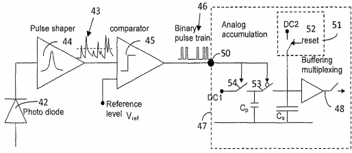 |
| 2009 | US8198577 | Granted 20120612 | Analog X-ray photon counting pixel The digital count as signal of a particle or photon counting pixels is store in a multi-level analog fashion. This analog function is made non-linear so as to exploit the difference in noise floor in the presence of photon shot noise. | 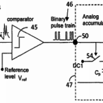 |
| 2008 | US7564022 | Granted 20090721 | Pixel with time gating function. “real” photodiodes bordered/interleaved with biasing diodes. When a biasing diode is at high potential, is steals away the photocharges of the real diodes; when the biasing diodes are al low potential, the real diodes are at max sensitivity. As this switching is effectively the modulation of the extension of the depletion layers, or of equipotential lines, it happens at very short time scales. It can be applied to optical/charge domain time gating of a light input; it can be applied to demodulation of optical inputs; it can be applied to time-of-flight imaging |  |
List of granted patents of Caeleste